
Raman Advantage — Technical Analysis Comparison
2025-12-12
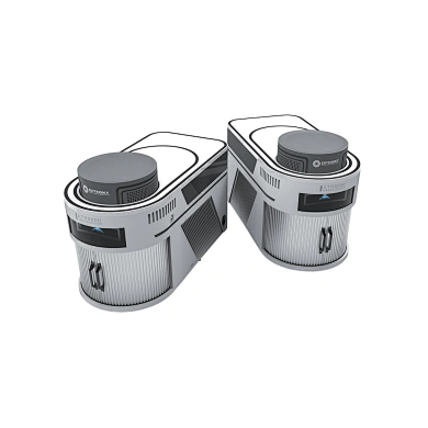
Why Choose Raman Spectroscopy?
Typically, Raman spectra (including peak positions and relative intensities) provide a unique chemical fingerprint of a substance, enabling its identification and differentiation from other materials. Actual measured Raman spectra are often complex, making it relatively difficult to determine unknown substances through peak assignment alone. However, by searching a Raman spectral database for matching results, unknown substances can be quickly identified.
Typically, Raman spectra (including peak positions and relative intensities) provide a unique chemical fingerprint of a substance, enabling its identification and differentiation from other materials. Actual measured Raman spectra are often complex, making it relatively difficult to determine unknown substances through peak assignment alone. However, by searching a Raman spectral database for matching results, unknown substances can be quickly identified.
What Are the Advantages of Raman Compared to Other Techniques?
Comparison with Fourier Transform Infrared (FTIR) Microscopy
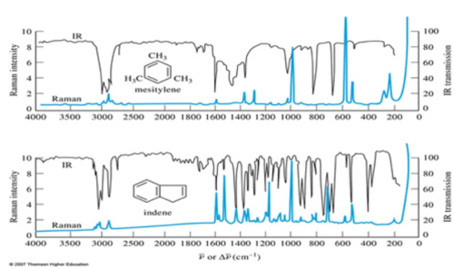
Raman spectroscopy is often compared with FTIR spectroscopy, which is considered the gold standard for molecular spectroscopy. The two techniques are complementary.
Advantages of Raman over IR:
-
Raman spectroscopy avoids many interferences from solvents, cells, and sample preparation methods.
-
Better selectivity, as Raman peaks are narrower.
-
Raman spectroscopy enables depolarization studies, which can enhance effects in certain cases.
-
Raman spectroscopy can detect vibration modes that are inactive in IR.
Comparison with X-Ray Diffraction (XRD)
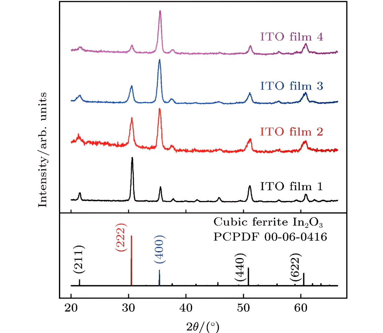
These two techniques are complementary in evaluating the crystal structure of materials.
Advantages of Raman over XRD:
Advantages of Raman over XRD:
-
Raman spectroscopy can measure both crystalline and amorphous materials, as well as perform single-particle analysis.
-
Easier control of environmental conditions: non-vacuum, heating/cooling/relative humidity, controlled stages.
-
Smaller footprint.
Comparison with Electron Microscopy
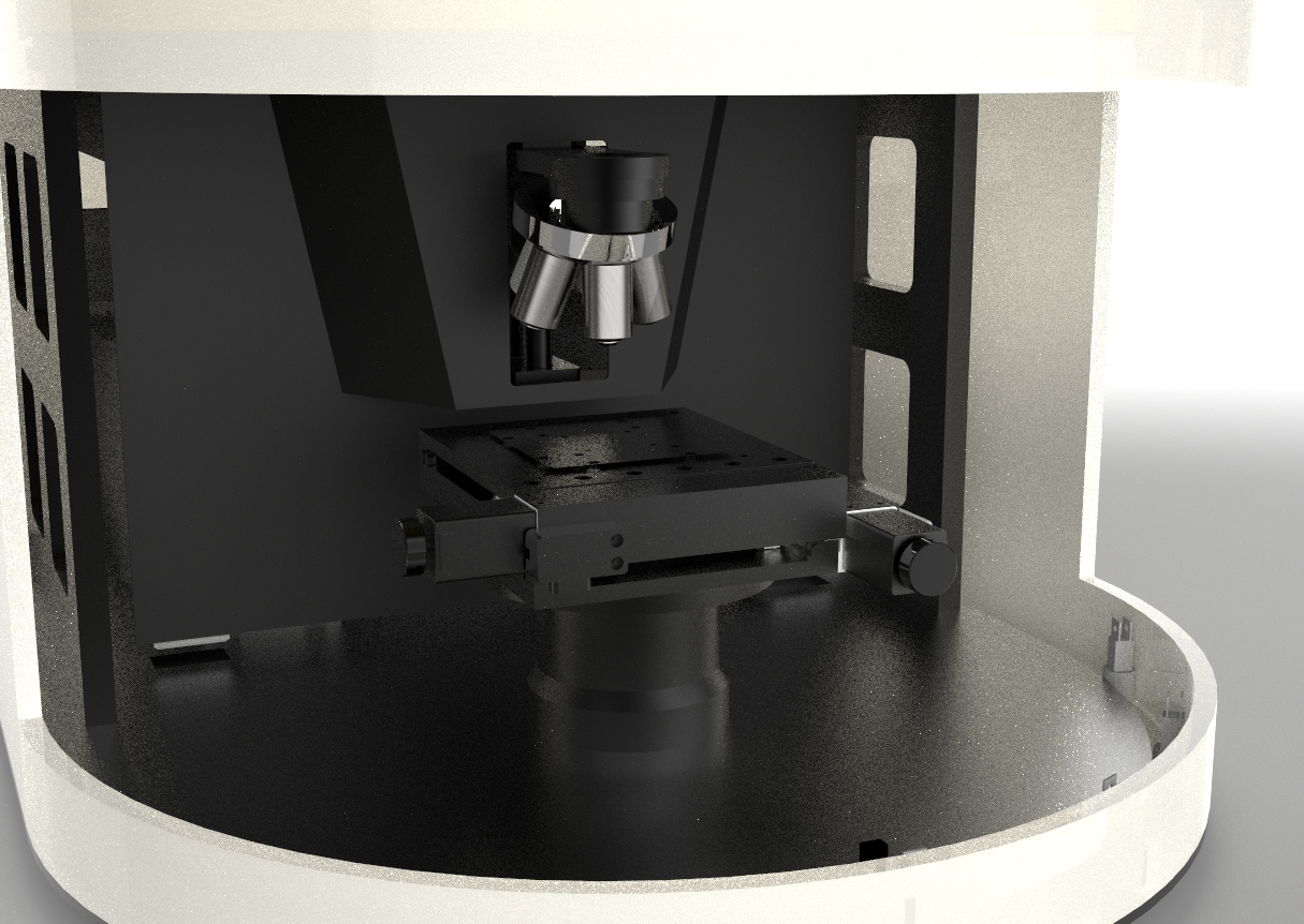
There are not many similarities between these two microscopy types. Both electron microscopy and optical microscopy are technical devices used to visualize physical and chemical structures too small to be seen by the naked eye, with relevant applications in biology and materials science. Generally, Raman microscopy and electron microscopy have different application areas and are complementary.
Advantages of Raman microscopy:
-
No sample preparation required.
-
Easier control of environmental conditions: non-vacuum, heating/cooling/relative humidity, controlled stages.
-
Faster analysis speed and high sample throughput.
-
Quick startup, with preparation for analysis in less than 10 minutes.
-
Capable of measuring multilayer samples and having a smaller footprint.
Follow us for more cutting-edge applications and solutions in Raman technology!
Email: [email protected]
Email: [email protected]
Raman Spectroscopy: The "Structural Tool" for Biomass Electrode R&D
Application Case | Online Raman PAT for Rapid Detection of Camellia Oil Adulteration
Related Article

Discover the Optosky ATR1600 ultra-micro Raman spectrometer—a 210g pocket-sized device for on-site, non-destructive gemstone identification. With a 20,000+ substance spectral library, dedicated jewelry edition, Bluetooth smartphone APP, and PDF reporting, it enables rapid screening of natural, synthetic, and treated gemstones at exhibitions, pawnshops, and markets.
ATR1600: The 210g Pocket Raman Gem Identifier
Explore how micro-confocal Raman spectroscopy, combined with SERS, enables rapid, non-destructive, molecular-level screening of veterinary drug residues such as malachite green, enrofloxacin, and chloramphenicol in aquatic products. Learn how Optosky’s ATR8100 supports microscopic localization, multi-wavelength excitation, mapping imaging, and portable on-site testing—while clarifying its role alongside LC-MS/MS confirmation.
Applications | Micro-Raman Drug Residue Screening in Seafood
Discover how Raman spectroscopy enables label‑free cancer diagnosis by reading molecular fingerprints of cells. From key Raman peaks and AI‑powered classification to the ATR8800 confocal platform, this article explores the frontiers, challenges, and clinical potential of Raman‑based cancer detection.
How Raman Spectroscopy Sees Through Cancer Cells: Label‑Free Cancer Diagnosis
Optosky successfully delivered and commissioned multiple ATP9100 field spectroradiometers at a university in Northwest China. The project included installation, performance verification, and on‑site training – supporting agricultural remote sensing, ecological monitoring, and geological surveys while building a standardized spectral research platform.
Case Study | ATP9100 Acceptance at Northwest University