
Application recommendation | Application of SM200 and its series film thickness gauges in thin film detection
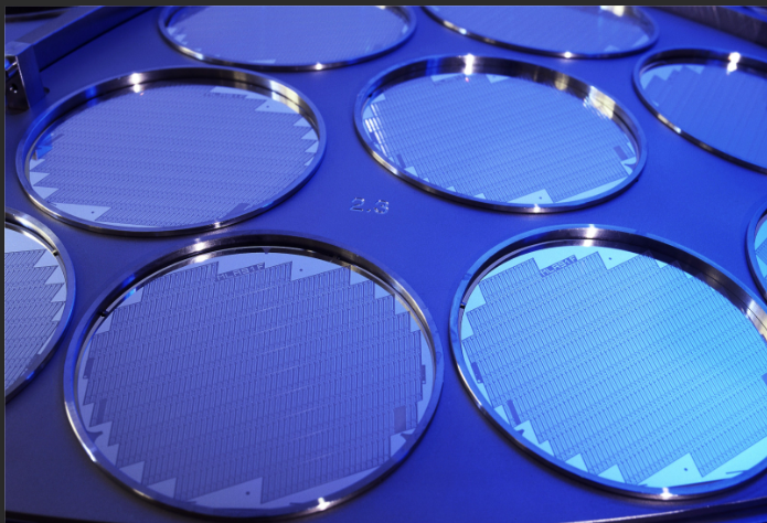
The thin film structure is a special form. Its size in the thickness direction is small and can only be measured microscopically. Due to the sudden change of the thin film structure at the interface, it has different properties from ordinary structures. Maxwell's "On Electricity and Magnetism" published in the 19th century laid the theoretical foundation for the thin film problem. In order to obtain excellent thin film performance, we need to accurately control the thickness parameters of the thin film so that the thin film device can work normally. Thin film detection technology has been widely developed in recent years, mainly including contact measurement methods, quartz crystal oscillation method, ellipsometry, reflection spectroscopy, white light spectroscopy, etc.
- Contact test
The probe method is a typical contact measurement method that uses the vertical offset generated when the probe moves on the film surface to measure the film thickness. The step meter is a typical application of this method. When using this method, steps must be made on the film. The substrate serves as the lower surface of the step and the film serves as the upper surface of the step. The probe contacts the surface of the film and completes the measurement according to the step. Under this measurement method, the film to be measured needs to be made steps first, have caused damage to many films, and scratches may be produced on the surface of the film during the contact process, resulting in slow measurement speed.
2. Quartz crystal oscillation method
The quartz crystal oscillation method mainly uses the piezoelectric effect and mass load effect of the quartz crystal to measure the film thickness by measuring the change in its natural resonant frequency. The resonant frequency of the quartz crystal piezoelectric effect is f=N/d, where f is the natural frequency of the quartz crystal, N is the frequency constant, and d is the crystal thickness. The quartz crystal oscillation method has matured after decades of development and is widely used in real-time online measurements.
3. Elliptical polarization method
The elliptical polarization method is based on the polarization phenomenon that occurs when polarized light is reflected on a film. When the component of polarized light is reflected by the sample surface, the polarization state will change. The elliptical polarization method uses the change of polarization state to calculate the optical constants of the film, mainly by calculating the reflection coefficient amplitude ratio and phase difference of the two components. The most widely used spectral ellipsometry system at present is a typical multi-wavelength solution. The measured ellipsometry parameters are inverted and optimized for fitting to obtain the film parameters. Ellipsometry has extremely high sensitivity and is especially suitable for measuring ultra-thin films and can measure quickly. However, due to excessive sensitivity, the non-uniformity of the film, sample surface, model differences, etc. will affect the accuracy of its measurement. The complexity, price, and computational complexity of the instrument also limit its widespread application.
4. Reflection spectroscopy
Reflection spectroscopy uses the reflectivity of the film to calculate the optical constants of the film, and is the most commonly used instrument for measuring films. The measurement principle is that light is incident on the film structure and reflected. A spectrometer is used to collect the reflection spectrum in a wide band, and the reflectance curve is calculated through a standard sample. Finally, the curve is optimized and fitted with the theoretical model to accurately solve the film parameters. Reflection spectroscopy has a wide measurement range and a simple testing process.
5. White light spectral interference method
This method mainly uses the interference principle of light and the principle of spectral splitting, and uses the interference intensity of light at different wavelengths to solve the problem. The light emitted from the light source is divided into two beams through the dichroic prism, one of which is incident on the reference mirror, and the other is incident on the surface of the measurement sample. Both beams of light are reflected and incident on the dichroic prism. At this time, the two beams of light will interfere. The interference light is collected by the spectrometer to obtain the white light spectrum interference signal. The film properties are obtained by analyzing its interference signal. The testing process is simple and has high accuracy.
As a leader in domestic spectroscopy companies, Optosky is committed to the development of domestic instruments. We also focus on launching optical film thickness instruments such as SM series, which are widely used in semiconductor coatings, photoresist films, nitride layers, polysilicon, etc. It is developed based on the principle of film reflected light interference. It uses light with a wavelength of 200-1700nm to be incident on the surface of the film. If the film has a certain degree of projection instrument, can calculate the thickness of the film based on the interference spectrum reflected back. The maximum thickness mapping range reaches 1nm-250um.
Instrument introduction
SM200 optical film thickness measurement mapping instrument
Non-contact, non-destructive testing.
Ultra-long life light source, higher luminous efficiency (light source can be customized).
Desktop distributed design, rich applicable scenarios.
Low maintenance cost and easy maintenance.
SM230 automatic optical film thickness scanning mapping instrument
Non-contact, non-destructive testing.
The surveying and mapping speed is fast and supports multi-point surveying and mapping point map drawing.
Supports drawing 2D/3D thickness distribution of samples.
High-precision, long-life 3-axis rotating platform.
SM280 microscope-based film thickness mapping instrument
Non-contact, non-destructive testing system.
Integrated live camera to monitor measurement points.
Equipped with a microscope objective to support detection of small-sized samples.
The software interface is intuitive, easy to operate and saves time.
Applications
- Application of film thickness measuring instrument in a certain crystal oscillator industry
The crystal oscillator industry generally uses the quartz oscillation method to test film thickness. For relatively thin films (a few microns and below), the accuracy usually does not meet the requirements.
A certain crystal oscillator industry used our instruments to conduct film thickness tests and obtained good results.
- Application of film thickness measuring instrument in silicon dioxide measurement
Silicon dioxide films have been widely used in the fields of semiconductors, microwaves, optoelectronics, optical devices, and thin film sensors due to their excellent properties. Therefore, it is very necessary to monitor and control their film thickness.
Test Results
|
Material |
Sample 1 (nm) |
Sample 2 (nm) |
Sample 3 (nm) |
Sample 4 (nm) |
Sample 5 (nm) |
Sample 6 (nm) |
|
Truth value (nm) |
120 |
69 |
45 |
35 |
12 |
110 |
|
Test 1 |
120.37 |
71.11 |
46 |
35 |
8.48 |
105.28 |
|
Test2 |
120.44 |
71.02 |
46 |
35 |
8.48 |
105.12 |
|
Test 3 |
120.3 |
71.19 |
46 |
35 |
8.36 |
105.22 |
|
Test4 |
120.42 |
71.06 |
46 |
35 |
8.36 |
105.19 |
|
Test 5 |
120.4 |
71 |
46 |
35 |
8.37 |
105.21 |
|
Repeatability |
0.14 |
0.19 |
0 |
0 |
0.12 |
0.16 |
|
Average value |
120.39 |
71.07 |
46 |
35 |
8.41 |
105.21 |
|
Accuracy |
0.39 |
2.07 |
1 |
0 |
3.52 |
4.8 |
(3) Application of film thickness measuring instrument on parylene coating
Parylene coating is widely used in PCB boards and related electronic device coatings. It has excellent electrical insulation and protection properties and is the most effective moisture-proof, mildew-proof, anti-corrosion and anti-salt spray coating material in the world.
Test Results
|
Sample name |
Film thickness (nm) |
Sample name |
Film thickness (nm) |
Sample name |
Film thickness (nm) |
Sample name |
Film thickness (nm) |
|
1029-1 |
30.44 |
1035-1 |
31.49 |
1039-1 |
30.42 |
1049-1 |
30.47 |
|
1029-2 |
30.43 |
1035-2 |
32.54 |
1039-2 |
30.44 |
1049-2 |
30.48 |
|
1029-3 |
30.40 |
1035-3 |
31.49 |
1039-3 |
30.45 |
1049-3 |
30.41 |
|
1029-4 |
30.42 |
1035-4 |
32.56 |
1039-4 |
30.43 |
1049-4 |
30.45 |
(4)Testing of PET film
The characteristic of PET reflective film is that the film has excellent optical properties and can be used in high-end vacuum aluminum plating and other products to achieve good results. The PET film is now tested.
Test Results
|
Sample number |
Number of measurements |
A (um) |
B (um) |
C (um) |
D (um) |
E (um) |
|
#1 |
1 |
24.71 |
24.5 |
25.59 |
25.45 |
25.53 |
|
2 |
24.97 |
24.52 |
25.07 |
24.93 |
25.79 |
|
|
3 |
24.44 |
24.52 |
25.59 |
25.19 |
25.52 |
|
|
4 |
24.97 |
24.5 |
25.59 |
25.71 |
25.79 |
|
|
5 |
24.45 |
24.58 |
25.33 |
25.45 |
25.52 |
|
|
Average value |
24.71 |
24.51 |
25.44 |
25.35 |
25.63 |
|
|
#2 |
1 |
25.89 |
25.65 |
25.23 |
23.45 |
25.56 |
|
2 |
25.64 |
25.39 |
25.55 |
23.19 |
25.82 |
|
|
3 |
25.63 |
25.65 |
24.74 |
23.72 |
25.56 |
|
|
4 |
25.11 |
25.39 |
25.28 |
23.19 |
25.82 |
|
|
5 |
25.63 |
25.65 |
25.55 |
23.98 |
25.82 |
|
|
Average value |
25.58 |
25.54 |
25.27 |
23.51 |
2572 |
|
|
#3 |
1 |
25.89 |
25.8 |
25.35 |
25.63 |
25.16 |
|
2 |
25.63 |
26.32 |
25.38 |
25.25 |
25.94 |
|
|
3 |
25.89 |
26.07 |
25.41 |
25.46 |
25.68 |
|
|
4 |
25.63 |
25.8 |
25.33 |
25.48 |
25.68 |
|
|
5 |
26.15 |
26.32 |
25.22 |
25.33 |
25.41 |
|
|
Average value |
25.84 |
26.06 |
25.34 |
25.43 |
25.57 |
Using a film thickness measuring instrument to test the PET film, the stability is good and the difference with the customer's true value is small.
Instrument parameters
SM series optical film thickness measuring instrument
|
Model |
SM-LUV |
SM-HUV |
SM |
SM-NIR |
|
General specifications |
||||
|
Spectral range |
200nm-1000nm |
200nm-1000nm |
400nm-1000nm |
900nm-1700nm |
|
Light source |
Deuterium-halogen combination lamp |
Tungsten halogen lamp |
||
|
Measurement specifications |
||||
|
Thickness range1 |
5nm-10um |
5nm-30um |
20nm-60um |
100nm-250um |
|
Accuracy2 |
±2nm or 0.2% |
±3nm or 0.4% |
||
|
Incidence angle |
90° |
|||
|
Film thickness layers |
1~3 |
|||
|
Sample material |
Transparent or translucent film |
|||
|
Measurement mode |
Single-point measurement/multi-point measurement/automatic measurement |
|||
|
Spot size3 |
2mm |
|||
|
Sample size |
Diameter from 1mm to 300mm or larger |
|||
|
Basic requirements |
||||
|
Operating system |
Windows10/11 |
|||
|
Indicator light |
Deuterium lamp indication, halogen lamp indication |
Halogen lamp indication |
||
|
Button |
Power button, deuterium lamp, halogen lamp |
Power button, Halogen light switch |
||
|
External interface |
Power outlet, USB 2.0, RJ45 |
|||
|
Movable stroke |
150mm*360° |
|||
|
Material |
Aluminum alloy |
|||
|
Power supply |
100~240VAC, 50~60Hz |
|||
|
Packing list |
Host, measurement platform, power cord, communication cable, optical probe, Y-shaped optical fiber |
|||
|
Remarks: 1. Depends on the material; 2. Whichever is larger depends on the material; 3. Optional to 20um |
||||
Summarize
The SM series film thickness measuring instrument adopts the principle of thin film reflected light interference and can be widely used in film thickness testing in semiconductor, photoresist, crystal oscillator, polysilicon, nitride layer and other industries. The test is non-destructive, fast, accurate and has a wide range of application scenarios. At the same time, customized measurements can be made according to user needs. If you are interested in the above solutions or have other film thickness application scenarios, or want to know more about the design details, please call us for consultation.