
How is the Raman spectrometer of optosky used in optics?
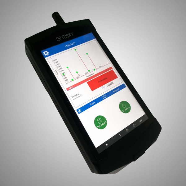
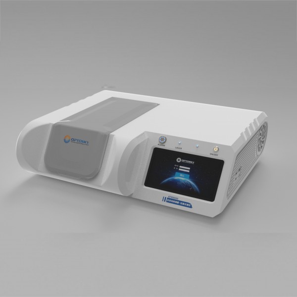
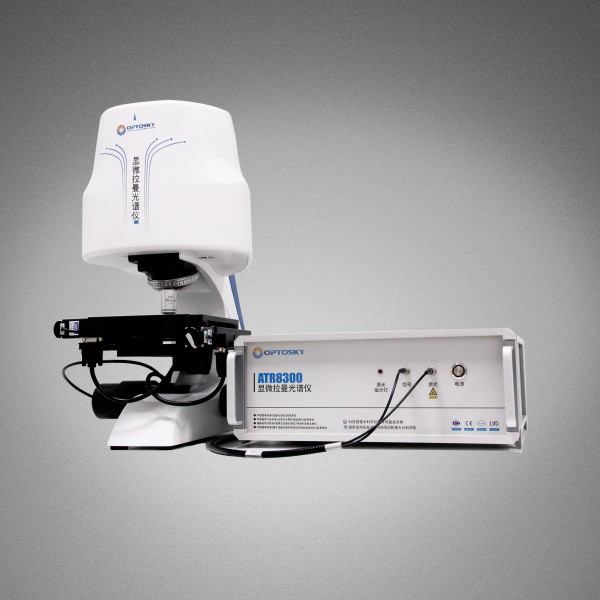
Optical spectroscopy has played a key role in the development of modern physics, from the early confirmation of quantum mechanics predictions of the spectrum of hydrogen to the observation of stars and interplanetary matter by astronomers refining their theory of the universe. Today, optical spectroscopy has become a routine method for the physicists and the astronomers, but also gained acceptance with chemists, biologists and metallurgists, amongst others.
Established in 2004, Optosky has secured its position as a world-leading manufacturer of measuring and analytical devices and supplies a vast array of sophisticated products into key markets including: automotive, biotechnology, environmental, medical, semiconductor, energy, pharmaceutical, and food science.
At the heart of an optical spectroscopy apparatus, the single device most closely associated with spectroscopic performance is the diffraction grating. It is therefore no surprise to see that the study and manufacture of diffraction gratings remain the domain of excellence of Optosky Photonice Inc. and a select few competitors worldwide.
To manufacture gratings of the highest quality, Optosky benefits from the largest dedicated commercial clean rooms equipped with both ruling engines and holographic exposure systems, and with the advanced metrology necessary to continuously improve the production processes (atomic force microscope, ultra high resolution monochromators, efficiency meters, ellipsometers...). On site vacuum testing is available for UV applications, together with a family of ion etching reactors to effect a controlled transfer of the gratings profile into the blank.
The quality of the substrate on which the grating structure is ruled or recorded requires high performance polishing, and Optosky realises this task internally for advanced applications. A dedicated chemical lab completes the gratings technical core of Optosky, improving photo resist definitions, cleaning processes and developing new solutions like oriented crystal etching and injection moulding.
Around the gratings, opto-mechanical designs result in the famous Optosky Photonic Inc. spectrometers, using computer aided tools to improve the productivity and tracability of the results. CCD detectors have gained acceptance thanks to their flexibility and price advantage. Optosky electronics skill centre pioneers the use of CCD technology for optical spectroscopy, developing high quantum efficiency cameras with ultra fast gating.
Finally, software development has become a major technology for Optosky Photonic Inc. in order to fully exploit the potential of digital data manipulation, through advanced algorithms for signal enhancement, multivariate detection or chemiometrics interpretations.
Each year the Optosky Photonic Inc. teams are granted more than 10 patents in China. You won't be regrets by Optosky.
What is the handheld Raman spectrometer of optosky?
How many advantagesof Raman ID applied to pharmaceutical industry?
Related Article