
Raman Spectroscopy and its Most Common Applications
Raman spectroscopy is a versatile tool that can be extended to cover any non-destructive analysis of chemical structure at a microscopic scale with imaging. Both qualitative and quantitative analysis can be performed by this technique, which is a rapid and convenient method for characterizing solids, liquids, gels, gases, slurry or powders, with respect to their chemical composition and structure.
List of Important Applications
The following are some important areas which use Raman spectroscopy to great effect.
Pharmaceutical Agents and Cosmetic Products
- The distribution of a compound within a tablet
- The uniformity of a blend
- High throughput screening
- The concentration of an API
- Testing the content and purity of a powder
- Verifying raw material quality
- Detecting polymorphism
- Analysis of crystalline structure
- Identification of contaminants
- Conducting in vivo analysis
- Skin depth studies
- Assaying the dose and uniformity of content
- Studying chemical combinations
Geology and Mineralogy
- Identification of various minerals and precious/semiprecious stones
- Analyzing fluid inclusions
- Studying the distribution of minerals and phases within a section of rock
- Analyzing phase transitions
- Studying the behavior of minerals under harsh conditions
- Identifying chondrite or achondrite meteorites
Carbon Materials
- Study of single-walled carbon nanotubes (SWCNTs)
- Analyzing the purity and measuring the electrical properties of carbon nanotubes (CNTs)
- Study of sp2 and sp3 structure in carbon materials
- Testing hard disk drives
- Analysis of the coating properties of diamond- like carbon (DLC)
- Detection of defects or disorder in carbon materials
- Testing diamond quality and place of origin
- Measuring the electrical properties and the number of layers of 2D materials like graphene
Semiconductors
- Identifying and describing inherent strain and stress of the molecular or chemical structure
- Assaying the purity
- Analysis of the composition of an alloy
- Identifying contaminants
- Studying the structure of a superlattice
- Analyzing defects in a structure
- Characterization of heterostructures
- Study of doping effects
- Microanalysis of photoluminescence
- Studying the electrical properties of 2D transition metal dichalcogenides such as MoS, WSe, WSe, and phosphorene
Life Sciences
- Analysis of biocompatibility of a material
- Analysis of nucleic acids
- Study of interactions between drugs and cells
- Photodynamic therapy (PDT)
- Analyzing metabolic accumulations of a substance or compounds
- Diagnosis of disease
- Analysis of individual cells
- Cell sorting applications
- Analyzing the features of biomolecules
- Study of bone structure
Discrimination of Different Phases and Polymorphs of a Material
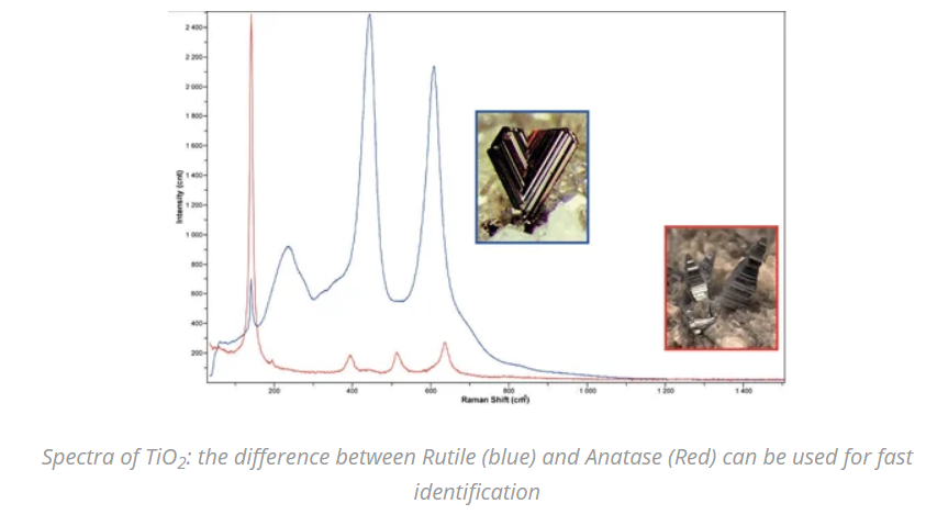
Raman scattering shows variations depending on the phase of the materials analyzed, and the presence of polymorphisms and solid structure, even if the materials themselves have the same chemical formulae. In such cases, the spectra are different because of their different phase and crystalline structure.
The spectrum often shows phase changes quite clearly, but this is not the case with other differences in structure of the material, such as polymorphism. These therefore are manifested as faint differences in spectra. A high resolution of the spectrum is necessary in these cases to be able to describe such small alterations with any degree of confidence
Analysis of Crystallinity of a Material
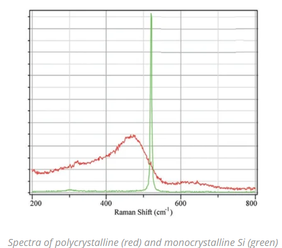
Raman scattering usually shows considerable variation with the degree to which the structure of a sample is crystalline, generating a spectrum with sharp high Raman peaks for crystals on the one hand, but broader and lower peaks with amorphous materials on the other. Thus, the completely amorphous and completely crystalline states may be taken to be at the extremes of the spectrum.
If a substance with an intermediate state is imaged by Raman spectroscopy, the spectrum will have peaks of intensity and width which fall in between these extremes. It can be difficult to discriminate between such characteristics beyond doubt without the ability to achieve high spectral resolution.
Software designed for peak fitting is often used in tandem with Raman spectroscopy in order to obtain accurate calculations of the width and intensity of the spectral peaks. These are subjected to calibration and are compared with the results obtained from other methods to provide quantitative measurements of the crystalline nature of a material. When Raman maps are analyzed in the same way, images are generated which represent the degree of crystallinity of the specimen.
ATR8800 Raman Imaging Technology
Raman : Applications
Related Article