
Application of Raman Spectroscopy in Detecting the Number of Graphene Layers
author: Otis
2022-09-29
What is Raman Spectroscopy?
Raman spectroscopy is a versatile, non-destructive technique based on the interaction of light with chemical bonds within a material that yields detailed information about chemical structure, phases and polymorphs, crystallinity and molecular interactions. Raman spectroscopy uses a monochromatic laser to probe materials, usually at visible or near-infrared wavelengths. Raman is a light scattering technique in which molecules scatter incident light from a high-intensity laser source. When a sample is irradiated, most of the light is scattered with no change in energy - this is called Rayleigh scattering. However, a small fraction of photons are scattered with the loss or gain of energy of the molecular vibrations - a phenomenon known as the Raman effect or Raman scattering. The energy of these vibrations is specific to the composition and structure of the molecule, which is why Raman is known as a chemical fingerprinting technique. Highly sensitive detectors and spectrometers are used to produce detailed and informative spectra from the collected light. Raman spectra are characterized by a number of peaks that show the intensity and wavelength position of the Raman scattered light. Each peak corresponds to a specific molecular bond vibration, including individual bonds such as C-C, C=C, N-O, C-H, etc.
Raman and graphene layers
Graphene is a unique material that contains single molecular layers of highly crystalline graphite. This material, first reported in 2004, represents the basic structural elements of carbon isomers, including carbon nanotubes, graphite and fullerenes.
Graphene has excellent electron transport properties, making it a promising material for future nanoelectronic devices. The material also has high thermal conductivity and high mechanical strength, approximately 200 times that of steel. It is also used in the development of ultrafast nanoscale transistors that operate in the terahertz region. Because of its size and optical properties, graphene is not visible on most substrates.
However, it is often difficult to optically locate graphene, and in order to study graphene-based devices, it is important to distinguish the number of graphene layers and to quantify the effect of disorder on their properties. Raman microspectroscopy provides a suitable and reliable technique to determine these two properties. The high spectral and spatial resolution of Raman spectroscopy, combined with the high structural selectivity and nondestructive nature of the technique, has made it a standard characterization tool in the rapidly growing field of graphene.
Since the discovery of graphene, Raman spectroscopy has been widely used in the study of graphene, such as: identifying the number of layers, doping type, structural defects, interlayer stacking of carbon atoms, in-plane vibrations of SP 2 carbon atoms, etc. Therefore, using Raman spectroscopy to study graphene has unique advantages.
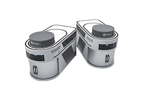
Optosky's research-grade micro Raman spectrometer ATR8800C, a series of micro Raman spectrometers, integrates up to four lasers and combines the advantages of both microscopy and Raman spectroscopy, making "what you see is what you measure" possible with a visual and precise positioning Raman detection platform. The visualization and precise positioning of the Raman detection platform enables the observer to detect the Raman signals of different surface states on the sample and display the morphology of the detected microregion on the computer simultaneously, which greatly facilitates the detection of Raman microregions. It has a good effect on the detection of graphene.
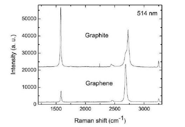
Fig.1 Comparison of Raman spectra of graphene and graphite
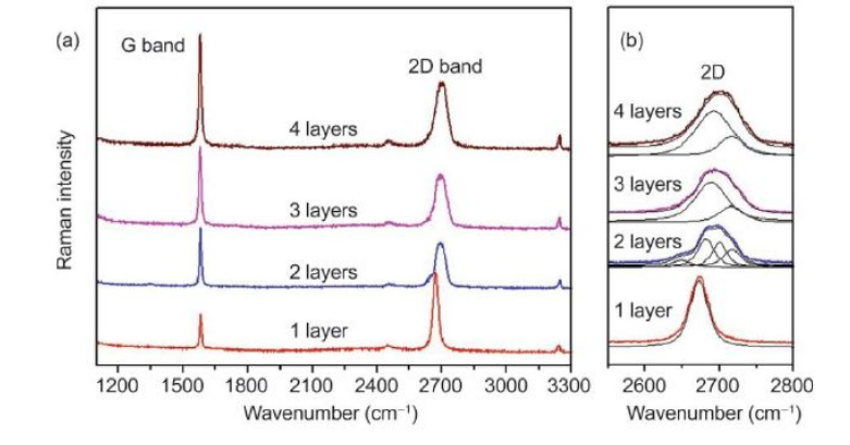
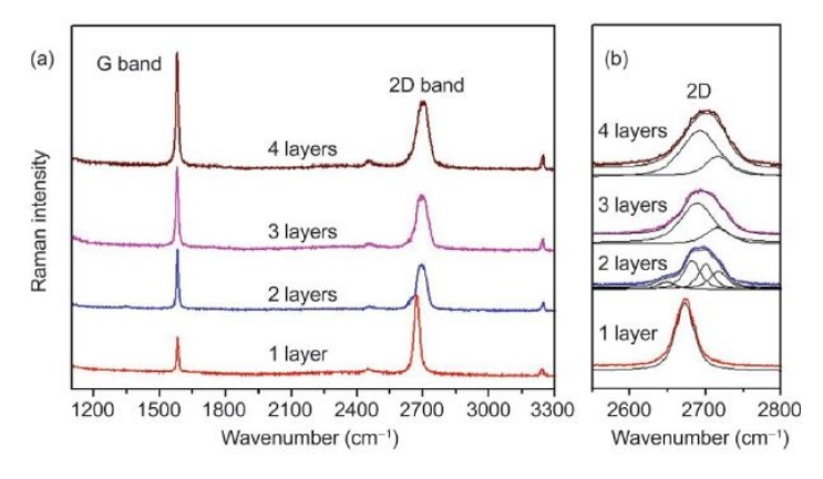
Fig.2 (a) Raman spectra of graphene with different layers [28]; (b) 2D peak fitting process of graphene with different layers
Fig.2 shows that the range of the full width at half maximum of graphene with different layers does not overlap, so the number of graphene layers can be determined by the full width at half maximum of the 2D peak.
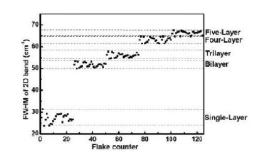
Fig. 3 The relationship between the 2D peak width at half maximum of the graphene Raman spectrum of graphene with different layers and the number of layers
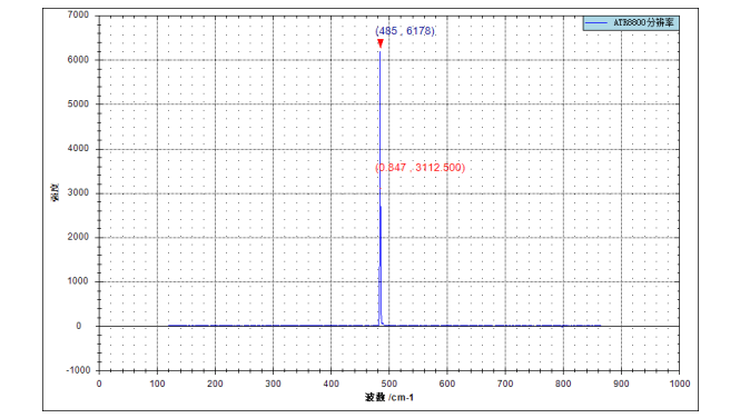
Fig. 4 The test results indicate: the resolution of the instrument reaches 0.847 cm-1, the test specification: according to the national standard "General Specification for Raman Spectrometer", the test equipment: ATR8800-FL510, the test light source: mercury-argon lamp, the collection line: 546.08
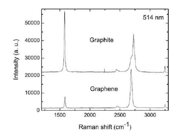
Fig5 Comparison of graphene and graphite Raman spectra
Application of Raman Spectroscopy in Single Crystal Silicon
What is a pinhole of confocal microscopes?
Related Article

Discover the Optosky ATR1600 ultra-micro Raman spectrometer—a 210g pocket-sized device for on-site, non-destructive gemstone identification. With a 20,000+ substance spectral library, dedicated jewelry edition, Bluetooth smartphone APP, and PDF reporting, it enables rapid screening of natural, synthetic, and treated gemstones at exhibitions, pawnshops, and markets.
ATR1600: The 210g Pocket Raman Gem Identifier
Explore how micro-confocal Raman spectroscopy, combined with SERS, enables rapid, non-destructive, molecular-level screening of veterinary drug residues such as malachite green, enrofloxacin, and chloramphenicol in aquatic products. Learn how Optosky’s ATR8100 supports microscopic localization, multi-wavelength excitation, mapping imaging, and portable on-site testing—while clarifying its role alongside LC-MS/MS confirmation.
Applications | Micro-Raman Drug Residue Screening in Seafood
Discover how Raman spectroscopy enables label‑free cancer diagnosis by reading molecular fingerprints of cells. From key Raman peaks and AI‑powered classification to the ATR8800 confocal platform, this article explores the frontiers, challenges, and clinical potential of Raman‑based cancer detection.
How Raman Spectroscopy Sees Through Cancer Cells: Label‑Free Cancer Diagnosis
Optosky successfully delivered and commissioned multiple ATP9100 field spectroradiometers at a university in Northwest China. The project included installation, performance verification, and on‑site training – supporting agricultural remote sensing, ecological monitoring, and geological surveys while building a standardized spectral research platform.
Case Study | ATP9100 Acceptance at Northwest University