
What is X-ray Fluorescence (XRF)
author: cily
2022-12-22
X-ray Fluorescence (XRF) is an analytical technique that uses the interaction of X-rays with a material to determine its elemental composition. XRF is suitable for solids, liquids and powders, and in most circumstances is non-destructive. XRF spectroscopy is an effective method for qualitative and quantitative analysis of material composition.
There are two main XRF methodologies - Energy Dispersive XRF (EDXRF) and Wavelength Dispersive XRF (WDXRF). Each method has its own advantages and disadvantages.
The range of detectable elements varies according to instrument configuration and set up, but typically EDXRF covers all elements from sodium (Na) to uranium (U), whilst WDXRF can extend this down to beryllium (Be). Concentrations can range from 100% down to ppm and in some cases sub-ppm levels. Limits of detection depend upon the specific element and the sample matrix, but as a general rule, heavier elements will have better detection limits.
XRF is widely used as a fast characterization tool in many analytical labs across the world, for applications as diverse as metallurgy, forensics, polymers, electronics, archaeology, environmental analysis, geology and mining.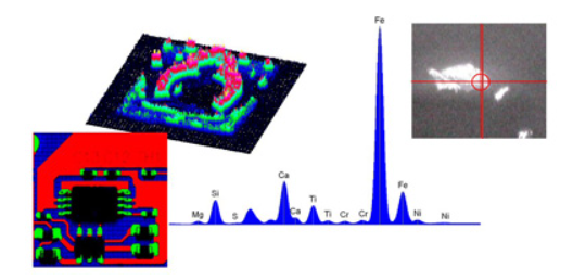
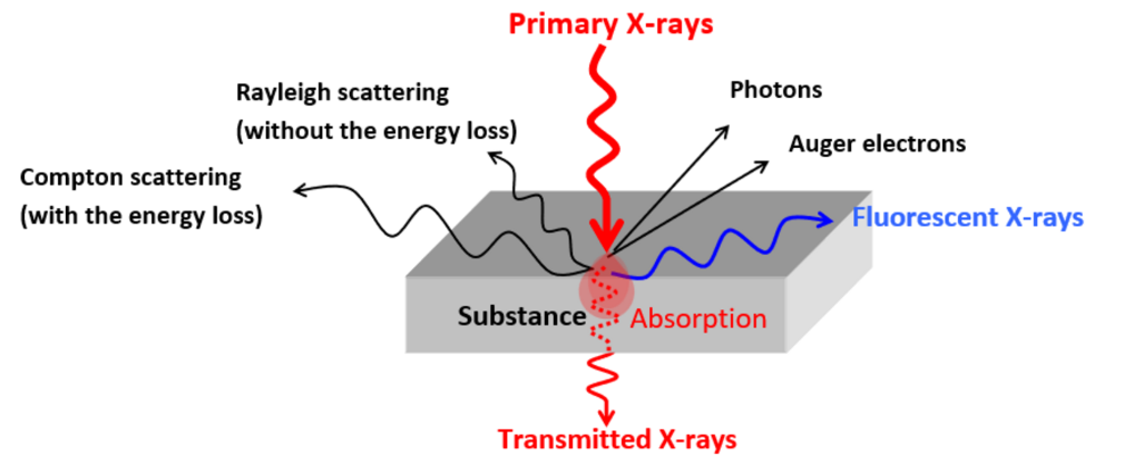
For example, interaction of X-rays with an atom with K, L and M shells could result in a hole forming in the K shell, which is then filled by an electron from the L shell or from the M shell. In either case, these are termed K transitions. Alternatively, a hole could be formed in the L shell, subsequently filled by an electron from the M shell (termed an L transition).
Thus, for a single element, a number of XRF peaks are possible, and typically these will all be present in the spectrum, with varying intensities. They form a characteristic fingerprint for a specific element.
In order to expel an electron from one of the orbitals, the X-ray energy must exceed the binding energy of that electron – however, if the X-ray energy is too high, then the coupling between X-ray and electron is inefficient, and only a few electrons will be knocked out. As the X-ray energy reduces, and approaches the electron binding energy, so the yield of expelled electrons increases. Just below this binding energy, a drop in absorption is observed, since the energy is not sufficient to emit electrons from that shell, and is too high in energy to emit electrons from the lower energy shells.
As explained in a previous section, not all the incident X-rays result in fluorescence. The fluorescence yield is the ratio of fluorescence X-rays to incident X-rays. The diagram below illustrates the K and L fluorescence yield as a function of atomic number, Z. It is clear that the yield for the light elements is very low, and this is reflected in achievable sensitivity for these elements.
The principle of the energy dispersive (ED) detector (such as the HORIBA Xerophy™) is based on the generation of electron-hole pairs in a semiconductor material (often silicon). An incident X-ray of energy EX, is absorbed by the detector material, and will cause one or more electron-hole pairs to form. The energy, EEHP, to do this is fixed for that particular material. The X-ray will form as many electron-hole pairs as its energy will allow: number of electron-hole pairs = EX / EEHP
Once this has occurred, the electrons are pulled off the detector, and the resulting current is proportional to the number of electron-hole pairs, which in itself is directly related to the X-ray energy.
This analysis process is repeated at a very high rate, and the results sorted into energy channels.
The X-rays are directed to a crystal, which diffracts the X-rays in different directions according to their wavelengths (energies).
On a sequential system a detector is placed at a fixed position, and the crystal is rotated so that different wavelengths are picked up by the detector. The XRF spectrum is built up point by point. In a simultaneous system, a number of crystal/detector units are used, so that a range of elements can be detected simultaneously.
The principal difference between ED and WDXRF techniques lies in the achievable energy (spectral) resolution. WDXRF systems can routinely provide working resolutions between 5 eV and 20 eV, depending on their set up, whereas EDXRF systems typically provide resolutions ranging from 150 eV to 300 eV or more, depending on the type of detector used.
The higher resolution of WDXRF provides advantages in reduced spectral overlaps, so that complex samples can be more accurately characterized. In addition, with high resolution backgrounds are reduced, providing improved detection limits and sensitivity.
However, the additional optical components of a WDXRF system (eg, diffracting crystal and collimators) means that it suffers from greatly reduced efficiency. Typically this is compensated for by high powered X-ray sources, which can have a significant impact on cost and ease of use. The additional optical components of WDXRF also effect the cost, and make for a relatively expensive instrument.
The final difference lies in spectral acquisition. With an EDXRF system such as XGT series an entire spectrum is acquired virtually simultaneously, so that elements from across most of the periodic table can be detected within a few seconds. With WDXRF spectrum acquisition is either made in a point by point fashion (which is extremely time consuming), or else has a very limited number of simultaneous detectors (which is an expensive option).
There are two main XRF methodologies - Energy Dispersive XRF (EDXRF) and Wavelength Dispersive XRF (WDXRF). Each method has its own advantages and disadvantages.
The range of detectable elements varies according to instrument configuration and set up, but typically EDXRF covers all elements from sodium (Na) to uranium (U), whilst WDXRF can extend this down to beryllium (Be). Concentrations can range from 100% down to ppm and in some cases sub-ppm levels. Limits of detection depend upon the specific element and the sample matrix, but as a general rule, heavier elements will have better detection limits.
XRF is widely used as a fast characterization tool in many analytical labs across the world, for applications as diverse as metallurgy, forensics, polymers, electronics, archaeology, environmental analysis, geology and mining.
What is X-rays?
X-rays form part of the electromagnetic spectrum, and are characterized by energies lying between gamma and ultra-violet radiation (Figure 1). Wavelengths are typically in the range 0.01 to 10 nm, which is equivalent to energies of 125 keV to 0.125 keV.Interaction of X-rays with a Substance
When X-rays irradiate to a substance, some of the X-rays pass through the substance, and some are absorbed in the substance. The absorbed X-rays interact within the substance in atomic level and cause various phenomena such as scattering and releasing photons, electrons, and fluorescent X-raysMultiple Transitions
Since most atoms comprise a number of electron orbitals (eg, K shell, L shell, M shell) a number of possible fluorescent transitions are possible.For example, interaction of X-rays with an atom with K, L and M shells could result in a hole forming in the K shell, which is then filled by an electron from the L shell or from the M shell. In either case, these are termed K transitions. Alternatively, a hole could be formed in the L shell, subsequently filled by an electron from the M shell (termed an L transition).
Thus, for a single element, a number of XRF peaks are possible, and typically these will all be present in the spectrum, with varying intensities. They form a characteristic fingerprint for a specific element.
Intensity
The absorption of X-rays by a particular material varies according to energy of the X-rays. As a rule of thumb, low energy X-rays are absorbed more than high energy photons.In order to expel an electron from one of the orbitals, the X-ray energy must exceed the binding energy of that electron – however, if the X-ray energy is too high, then the coupling between X-ray and electron is inefficient, and only a few electrons will be knocked out. As the X-ray energy reduces, and approaches the electron binding energy, so the yield of expelled electrons increases. Just below this binding energy, a drop in absorption is observed, since the energy is not sufficient to emit electrons from that shell, and is too high in energy to emit electrons from the lower energy shells.
As explained in a previous section, not all the incident X-rays result in fluorescence. The fluorescence yield is the ratio of fluorescence X-rays to incident X-rays. The diagram below illustrates the K and L fluorescence yield as a function of atomic number, Z. It is clear that the yield for the light elements is very low, and this is reflected in achievable sensitivity for these elements.
Energy Dispersive XRF (EDXRF)
An energy dispersive detection system directly measures the different energies of the emitted X-rays from the sample. By counting and plotting the relative numbers of X-rays at each energy an XRF spectrum is generated.The principle of the energy dispersive (ED) detector (such as the HORIBA Xerophy™) is based on the generation of electron-hole pairs in a semiconductor material (often silicon). An incident X-ray of energy EX, is absorbed by the detector material, and will cause one or more electron-hole pairs to form. The energy, EEHP, to do this is fixed for that particular material. The X-ray will form as many electron-hole pairs as its energy will allow: number of electron-hole pairs = EX / EEHP
Once this has occurred, the electrons are pulled off the detector, and the resulting current is proportional to the number of electron-hole pairs, which in itself is directly related to the X-ray energy.
This analysis process is repeated at a very high rate, and the results sorted into energy channels.
Wavelength Dispersive XRF (WDXRF)
A wavelength dispersive detection system physically separates the X-rays according to their wavelengths.The X-rays are directed to a crystal, which diffracts the X-rays in different directions according to their wavelengths (energies).
On a sequential system a detector is placed at a fixed position, and the crystal is rotated so that different wavelengths are picked up by the detector. The XRF spectrum is built up point by point. In a simultaneous system, a number of crystal/detector units are used, so that a range of elements can be detected simultaneously.
The principal difference between ED and WDXRF techniques lies in the achievable energy (spectral) resolution. WDXRF systems can routinely provide working resolutions between 5 eV and 20 eV, depending on their set up, whereas EDXRF systems typically provide resolutions ranging from 150 eV to 300 eV or more, depending on the type of detector used.
The higher resolution of WDXRF provides advantages in reduced spectral overlaps, so that complex samples can be more accurately characterized. In addition, with high resolution backgrounds are reduced, providing improved detection limits and sensitivity.
However, the additional optical components of a WDXRF system (eg, diffracting crystal and collimators) means that it suffers from greatly reduced efficiency. Typically this is compensated for by high powered X-ray sources, which can have a significant impact on cost and ease of use. The additional optical components of WDXRF also effect the cost, and make for a relatively expensive instrument.
The final difference lies in spectral acquisition. With an EDXRF system such as XGT series an entire spectrum is acquired virtually simultaneously, so that elements from across most of the periodic table can be detected within a few seconds. With WDXRF spectrum acquisition is either made in a point by point fashion (which is extremely time consuming), or else has a very limited number of simultaneous detectors (which is an expensive option).
Key notes of XRF
Traditionally XRF has been a bulk technique with analysis spots in the region of several millimeters through to several centimeters. For inhomogeneous samples, X-ray Fluorescence Spectroscopy (micro-XRF) is suitable to get elemental distribution images on the samples.How is XRF used in industries?
Applications benefiting from HORIBA’s X-ray fluorescence technology include forensics, geology, materials, biology/medicine, electronics, archaeology, engine wear analysis, pharmaceutics, and RoHS/ELV compliance testing.Raman spectroscopic detection and analysis of Scutellaria baicalensis herbal tablets
What is the Raman microscope?
Related Article

Discover the Optosky ATR1600 ultra-micro Raman spectrometer—a 210g pocket-sized device for on-site, non-destructive gemstone identification. With a 20,000+ substance spectral library, dedicated jewelry edition, Bluetooth smartphone APP, and PDF reporting, it enables rapid screening of natural, synthetic, and treated gemstones at exhibitions, pawnshops, and markets.
ATR1600: The 210g Pocket Raman Gem Identifier
Explore how micro-confocal Raman spectroscopy, combined with SERS, enables rapid, non-destructive, molecular-level screening of veterinary drug residues such as malachite green, enrofloxacin, and chloramphenicol in aquatic products. Learn how Optosky’s ATR8100 supports microscopic localization, multi-wavelength excitation, mapping imaging, and portable on-site testing—while clarifying its role alongside LC-MS/MS confirmation.
Applications | Micro-Raman Drug Residue Screening in Seafood
Discover how Raman spectroscopy enables label‑free cancer diagnosis by reading molecular fingerprints of cells. From key Raman peaks and AI‑powered classification to the ATR8800 confocal platform, this article explores the frontiers, challenges, and clinical potential of Raman‑based cancer detection.
How Raman Spectroscopy Sees Through Cancer Cells: Label‑Free Cancer Diagnosis
Optosky successfully delivered and commissioned multiple ATP9100 field spectroradiometers at a university in Northwest China. The project included installation, performance verification, and on‑site training – supporting agricultural remote sensing, ecological monitoring, and geological surveys while building a standardized spectral research platform.
Case Study | ATP9100 Acceptance at Northwest University