
Raman Spectroscopy in Photovoltaic Materials Research
2024-09-23
With the growing global demand for energy and increasing environmental concerns, solar energy has garnered widespread attention as a clean and renewable resource. Photovoltaic materials, which are essential for converting sunlight into electricity, play a critical role in determining the efficiency, cost, and stability of solar cells. Research on photovoltaic materials involves various aspects such as material synthesis, structural optimization, defect control, doping regulation, and enhancing the stability of devices.
Raman spectroscopy is a characterization technique based on molecular vibration modes. By detecting the inelastic scattering of photons after interaction with material molecules, it provides valuable information on chemical bonds, structure, stress, and defects in materials. In photovoltaic research, Raman spectroscopy is widely used due to its non-destructive, high-resolution, and sensitive capabilities for analyzing materials ranging from monocrystalline silicon to emerging perovskite solar cells. Its unique ability to characterize microstructure, chemical composition, impurities, and defects makes it indispensable. This article will explore the specific applications of Raman spectroscopy in various solar cell materials, particularly its contributions to crystal structure characterization, defect analysis, and stress measurement.
Crystallinity
Crystallinity refers to the proportion of the crystalline regions within a material, describing the relative ratio of ordered crystal structures to disordered amorphous areas. In photovoltaic materials such as silicon-based solar cells, an increase in crystallinity often leads to enhanced carrier mobility and reduced recombination rates, which in turn improve the photoelectric conversion efficiency. Therefore, accurately assessing the crystallinity is a crucial step in optimizing solar cell materials. Raman spectroscopy effectively calculates crystallinity by analyzing the Raman spectral peaks corresponding to crystalline and amorphous phases, which is especially important for characterizing materials like polysilicon and amorphous silicon.
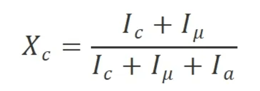
Raman spectroscopy detects different vibrational modes in crystalline and amorphous silicon, providing valuable crystallization information. Crystalline silicon (e.g., monocrystalline or polycrystalline silicon) typically exhibits a sharp, high-intensity Raman peak around 520 cm⁻¹, which corresponds to the phonon vibration modes of silicon atoms. Amorphous silicon, due to its disordered structure, shows a broader spectral band near 480 cm⁻¹. Additionally, microcrystalline silicon displays a characteristic peak around 510 cm⁻¹, which is broader than the crystalline silicon peak at 520 cm⁻¹. By calculating the intensity ratios of the peaks for crystalline, microcrystalline, and amorphous silicon, the crystallinity of the material can be quantified.
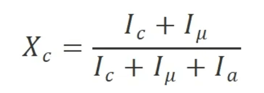
The formula for calculating crystallinity
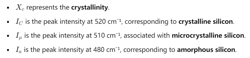

Figure 1 presents the typical Raman spectra from both sides of a solar cell, captured using excitation wavelengths of 514 nm and 633 nm.
Doping and Defect Characterization
Doping is a crucial method for regulating the electrical properties of photovoltaic materials. By introducing small amounts of impurity elements, the conductivity, band structure, and light absorption capabilities of materials can be fine-tuned. However, doping may also introduce defects that affect the efficiency of solar devices. Thanks to its sensitivity to lattice vibration modes, Raman spectroscopy can detect and analyze structural changes caused by doping, the local environment of the dopant atoms, and the generation of defects.
Raman Characteristics of Dopants
Raman spectroscopy can effectively characterize the location and distribution of dopants in photovoltaic materials by detecting their unique vibrational modes.
Silicon-Based Materials: In silicon solar cells, common dopants include phosphorus (n-type doping) and boron (p-type doping). Doping induces local stress fields and lattice mismatches, resulting in changes in the position, intensity, and width of Raman peaks. The doping of phosphorus and boron can cause slight shifts and broadening of the Si-Si bond Raman peak at 520 cm⁻¹. These changes allow for a quantitative analysis of doping concentration and stress field distribution.

Figure 2 (a-f) shows the characteristic peaks of microcrystalline silicon at varying boron doping concentrations. As the doping concentration increases, the characteristic peaks shift from 520 cm⁻¹ for crystalline silicon towards 480 cm⁻¹ for the amorphous phase. These measurements were taken using a 632.8 nm laser.
In perovskite solar cells, metal ions (e.g., lithium, sodium) or halide anions (e.g., bromine, chlorine) are commonly doped to regulate the bandgap and enhance the stability of the material. Doping ions typically alter the vibrational modes of the perovskite crystal, resulting in new Raman spectral peaks or shifts in existing ones. For instance, chlorine doping can cause changes in the I-Pb-I vibrational mode, reflecting crystal distortion after doping. This method of using Raman spectroscopy to detect shifts in vibrational modes is vital for optimizing the efficiency and durability of perovskite solar cells.

Figure 3 compares the Raman spectra of doped and undoped perovskite materials
Impact of Doping on Defects
During the doping process, structural defects such as vacancies, interstitial atoms, and dislocations may be introduced. These defects can negatively affect the carrier recombination rate in photovoltaic devices, reducing overall solar cell efficiency. Raman spectroscopy is a powerful tool for detecting these defects through peak broadening or shifts in peak position, providing insights into the material's structural integrity.
Vacancies and Interstitial Defects: Doping can introduce vacancies (e.g., Cd vacancies in CdTe) or interstitial atoms, causing localized instability in the crystal structure. Changes in Raman peak width reflect increased lattice disorder, allowing for the quantitative analysis of defect concentrations.
Dislocations and Grain Boundaries: In polycrystalline thin-film photovoltaic materials, doping may also induce dislocations and local stress concentrations near grain boundaries. These defects can also be observed through the broadening and shifting of Raman peaks, aiding in the optimization of the doping process.
Real-time Monitoring of Defect Formation During Doping
The non-destructive nature of Raman spectroscopy makes it ideal for real-time monitoring of defect formation and evolution during the doping process. For instance, in the production of CIGS thin-film photovoltaic devices, Raman spectroscopy can track the distribution changes of elements such as Cu, In, and Ga, and the corresponding defect formation. This provides valuable information on doping concentration and uniformity, which is critical for optimizing the process and improving the performance and uniformity of solar devices.
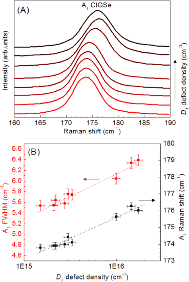
Figure 4 illustrates the relationship between the A1 peak position in the Raman spectrum of CIGS devices and defect density
Stress and Strain Measurement
During the manufacturing, packaging, and operation of photovoltaic materials, various mechanical stresses can affect the crystal structure and lead to performance degradation. Raman spectroscopy is a powerful tool for measuring internal stress and strain in materials by detecting shifts in Raman peaks (redshift or blueshift) to quantify the stress fields present.
Principle of Stress Measurement: When external stress is applied to a material, the lattice constant changes, causing alterations in the phonon vibration frequency observed in Raman scattering. For example, in silicon materials, compressive stress shifts the 520 cm⁻¹ Raman peak to higher wavenumbers, while tensile stress shifts it to lower wavenumbers. This shift can be quantified to precisely calculate the stress within the material.
Thin Film Stress: Thin-film photovoltaic materials, such as CIGS and CdTe, are often deposited on heterogeneous substrates, which introduces significant stress. Raman spectroscopy is used to monitor residual stress in the films and its effect on the performance of photovoltaic devices. For example, in CIGS thin films, shifts in the Raman peaks reveal stress gradients within the film, which is crucial for adjusting deposition processes to reduce stress and improve material performance.
Conclusion
The application of Raman spectroscopy in photovoltaic materials research spans from crystal structure characterization and defect analysis to stress and strain measurement. As solar technology advances, Raman spectroscopy will continue to play an irreplaceable role as a sensitive and efficient tool in the development of new materials and the optimization of device performance.
Facing the "chaos in tanker transportation", technology protects "food safety"
Raman Application in Diesel Detection
Related Article

Raman peaks don't lie — if you know how to read them.
Let's have a look!
Let's have a look!
Raman Characteristic Peaks – A Short Summary

Want to know details of ATR3100 Portable Raman Spectrometer Introduction ? Leading supplier - Optosky will share knowledge of portable Raman spectrometer , cooled CCD Raman , high‑sensitivity Raman for you. Click the link to get more information.
ATR3100 Portable Raman Spectrometer Introduction
Real‑world Raman mapping case study: analysing surface distribution of 4‑MBA, cortisol, DHEA, and dopamine using 785 nm excitation. See how flexible parameters, fluorescence suppression, and system stability enable reliable mapping results – with parallel sample verification for repeatability.
Applications | Raman Mapping in Practice: Surface Distribution Analysis of Four Molecular Samples

Optosky ATR8800 is a next-gen confocal micro-Raman imaging system with 0.35μm resolution, 2nm nanopositioning, and depth-of-field fusion. It delivers high-speed, non-destructive analysis for materials science, life sciences, and semiconductors.
Product Upgrade | ATR8800 Comprehensive Upgrade: Faster · More Precise · Sharper