
What Is Raman Spectroscopy Used For?
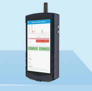
The application fields, in which Raman spectroscopy is used are vast. The article takes you to the various areas where Raman spectroscopy is used and valued better.
Uses of Raman Spectroscopy
There are a plethora of areas where Raman spectroscopy is used. They are mentioned as follows:
- Pharmaceuticals
- Cosmetics
- Geology
- Mineralogy
- Carbon materials
- Semiconductors
- Life sciences
- Transmission
- Optoelectronics
- Polymers
- Materials
- Nanomaterials
- In situ analysis
- Geology
- Forensics
- Food & beverage
- Environment
- Energy
- Corrosion
- Catalysis
- Biology
- AFM
- Art & museums
Biology
The Raman spectroscopy technique provides label free characterization of biochemistry with sub-micron optimal resolution. It is an utility in the areas of:
- Detection of disease
- Cell research
- Drug design and pharmaceutical materials
- Microbiology and cell-sorting
- Cosmetics and in vivo skin analysis
- Stents and implants
- Characterisation of drug-cell interactions
- Metabolic accretions
- Photodynamic therapy
- Bone structure
- DNA and RNA analyses
The following are the specific applications in biology:
- SERS (Surface Enhanced Raman Spectroscopy) analysis of single living lymphocytes
- Analysis of single bacterium cell
- Mapping of wheat grain kernel
- In vivo measurement of human skin
- High resolution SERS details thrombosis mechanism
- SERS for intracellular imaging
- Sperm nuclear DNA integrity
- Raman Spectroscopy imaging of Monkey brain tissue
- Investigation of microbes on a single cell level
- Investigation of atherosclerosis process through monitoring of cholesterol and free fatty acids
- In solid media, direct identification of clinically relevant microorganisms.
Art & Museums
- Raman spectroscopy is utilized in art and museums for the following purposes:
- Non-destructive and in-situ analysis of pigments
- Archaeometric analysis of ancient pottery
- Micro raman pigment analysis of wall paintings in church
Tip Enhanced Optical Spectroscopy (TEOS) & Tip Enhanced Raman Scattering (TERS)
- Characterization of molybdenum disulfide flakes using TEOS
- Characterization of carbon nanotubes using TERS
- Characterization of graphene raman spectrum using TERS
Carbon
- Raman spectroscopy is used in the following sectors related to carbon:
- Important forms of elemental carbon
- Raman spectra of hard carbon films used for derivation of physical parameters
- Information on carbon nanotubes like purity, electrical properties,
- Colored diamond investigation
- Raman spectroscopy of graphene
Catalysis
In situ characterization of heterogeneous catalytic reactions
Corrosion
Observation of oxidation kinetics on aluminium alloy surface with fluorescence mapping
Cosmetics
Raman mapping utilized in investigation of soap compound
Energy
Lithium-ion battery analysis
Environment
- Identification of air borne pollen
- Statistical, Morphological and chemical depiction of particles on cellulose nitrate filters in quality control
- Confocal Raman spectroscopy imaging with amalgamation of chemometric methods for environmental applications
The objectives fulfilled by the Raman spectroscopy include:
- Identification and validation of biological mechanisms behind the target or disease
- Identification of active molecules in the target
- Selection of candidate drugs and optimized properties for future developments
- Preclinical trials to document the safety of compound to enter into human trials
- Science of development, formulation and manufacturing of final drug product
- Ensuring the quality of durg and reduction of irrelevant products
- Defense of intellectual property
- Study of generics
- Fight against marketing of counterfeit
Semiconductors
- Raman imaging of of single gallium nitride nanowire
- Detection of strained silicon in MOSFETs
- Strain assessment in Si cap layer, which is deposited on a SiGe substrate
- Determination of Ge content in SiGe substrate
Conclusion
The use of Raman spectroscopy and its types are innumerable. Compared to UV-Vis spectroscopy, it has more sensitive usage, which is extremely important for the production of various industries.
(Suzhou Institute of Biomedical Engineering Technology, Chinese Academy of Sciences)Escherichia coli sample and Staphylococcus aureus Raman spectrum detection report on silver substrate
Test Report of Insulating Oil and Insulating Paper of Electrical Engineering College of Chongqing University
Related Article