
Spectrometer semiconductor Plasma process monitoring OES Endpoint detection etching
2025-11-04
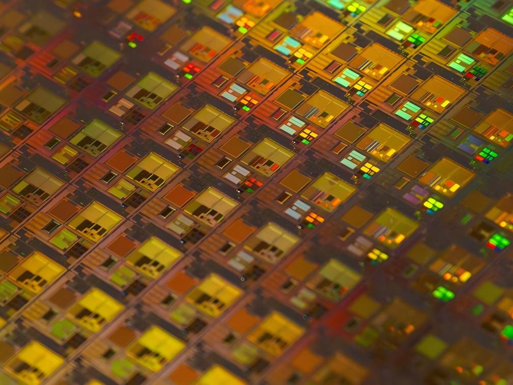
In semiconductor manufacturing – a field often regarded as the pinnacle of human industrial precision – a deviation of even a single nanometer or a one-second process error can drastically alter chip performance or scrap an entire production batch. Consequently, real-time, in-line, high-precision monitoring and control have become essential for ensuring production yield.
Spectrometers, leveraging their unique advantages, are increasingly becoming the indispensable "intelligent eyes" for precision analysis within the semiconductor industry chain.
Core Advantages over Traditional Spectrometers:
-
Flexibility & Easy Integration: By remotely transmitting light signals via optical fibers, the spectrometer main unit can be installed in a stable control room, while only the compact sampling probe accesses the equipment chamber or production line. This perfectly adapts to the complex internal structures and demanding installation environments of semiconductor tools.
-
Real-time, In-line Monitoring: Capable of continuous, rapid measurements, providing immediate feedback on process parameter changes. This establishes the data foundation for Advanced Process Control (APC) and Fault Detection and Classification (FDC), thereby improving yield and reducing waste.
-
High Precision & Reliability: Utilizing array detectors (e.g., CCD, CMOS) with no moving parts enables fast scanning speeds and high stability, meeting the extreme demands for measurement repeatability and reliability in semiconductor processes.
-
Multi-channel Simultaneous Analysis: A single spectrometer can connect to multiple sampling probes, enabling simultaneous monitoring of various points or different wavelength bands, thus enhancing equipment utilization and inspection efficiency.
Core Advantages over Traditional Spectrometers:
-
Flexibility & Easy Integration: By remotely transmitting light signals via optical fibers, the spectrometer main unit can be installed in a stable control room, while only the compact sampling probe accesses the equipment chamber or production line. This perfectly adapts to the complex internal structures and demanding installation environments of semiconductor tools.
-
Real-time, In-line Monitoring: Capable of continuous, rapid measurements, providing immediate feedback on process parameter changes. This establishes the data foundation for Advanced Process Control (APC) and Fault Detection and Classification (FDC), thereby improving yield and reducing waste.
-
High Precision & Reliability: Utilizing array detectors (e.g., CCD, CMOS) with no moving parts enables fast scanning speeds and high stability, meeting the extreme demands for measurement repeatability and reliability in semiconductor processes.
-
Multi-channel Simultaneous Analysis: A single spectrometer can connect to multiple sampling probes, enabling simultaneous monitoring of various points or different wavelength bands, thus enhancing equipment utilization and inspection efficiency.
Core Application Scenarios
The applications of fiber optic spectrometers span virtually all key stages of chip manufacturing, both front-end and back-end. Here are several of the most critical ones:
1. Plasma Process Monitoring (Dry Etching & Chemical Vapor Deposition)
Plasma is central to etching and thin-film deposition processes, and its state directly determines the process outcome. Real-time collection of plasma emission spectra (OES) via fiber optic spectrometers enables:
Endpoint Detection: In etching processes, when a specific material is completely etched, the intensity of its characteristic spectral line in the plasma changes abruptly. The spectrometer accurately captures this moment, automatically terminating the etch to prevent over-etching or under-etching – a core function for maintaining critical dimension accuracy.
Process State Monitoring: By analyzing the spectral intensities of active species (e.g., F, Cl, O, H) in the plasma, process stability can be monitored in real-time, and equipment anomalies (such as chamber micro-leaks, electrode aging, or gas ratio imbalances) can be diagnosed, enabling predictive maintenance.
2. Thin Film Thickness Measurement (Dielectric Layers, Photoresist, Metal Films, etc.)
Based on white-light interferometry principles, fiber optic spectrometers analyze the interference spectrum reflected from a thin film on a substrate, enabling non-contact, non-destructive, and precise calculation of film thickness (nanometer scale) and refractive index. This is widely applied for:
-
Measuring photoresist thickness on wafers to ensure accurate pattern transfer in lithography.
-
Monitoring the growth thickness of dielectric layers like silicon oxide and silicon nitride.
-
Measuring the thickness uniformity of various films deposited by CVD, PVD, and other processes.
3. Wafer Cleaning & Surface Treatment Monitoring
In cleaning baths, fiber optic spectrometers can monitor the concentration of cleaning solutions (e.g., SC1, SC2, HF). By analyzing the absorption spectra of specific chemical bonds in the IR or UV range, they can determine in real-time whether the active chemical components are within the specified process window, prompting timely replenishment or replacement to ensure consistent cleaning effectiveness and cost control.
4. LED & Semiconductor Laser Testing
-
In back-end manufacturing, fiber optic spectrometers are core instruments for optoelectronic characterization. They enable rapid measurement of key LED chip parameters:
-
Dominant Wavelength, Peak Wavelength, and Spectral Full Width at Half Maximum (FWHM): For assessing color characteristics.
-
Color Purity and Chromaticity Coordinates: Critical for display applications.
-
Optical Power and Luminous Efficiency: For evaluating performance.
Their high speed and non-destructive nature make them ideally suited for integration into Automated Test Equipment (ATE) for comprehensive testing and sorting (Binning).
Conclusion
As semiconductor technology nodes continue to shrink and third-generation semiconductor materials (like SiC, GaN) see broader application, the demands for process monitoring precision, speed, and reliability are intensifying. Fiber optic spectrometers, with their inherent flexibility, in-line capability, and high precision, perfectly align with these requirements, solidifying their role as a key tool empowering advanced manufacturing and enhancing production line yield and profitability.
Citrus chilling injury detection Online fruit quality inspection Non-destructive fruit testing
Spectral Analysis: Principles of LIF Technology and Applications of Spectrometers
Related Article

The ATP7810 is a wide-band, high-resolution infrared grating spectrometer covering up to 0.9–5 μm. Featuring a motorized rotating grating, multiple detector options (InGaAs/MCT), and flexible interfaces (SMA905 or free space, USB/UART control), it delivers high SNR and stability for absorption/reflection/transmission spectroscopy, laser wavelength testing, and fiber optic sensing.
New Product Recommendation | ATP7810 Ultra-Wide Range Infrared Spectrometer Series

This study uses the ATP5200P UV-Vis spectrometer to investigate xanthate adsorption on chalcopyrite surfaces. By analyzing absorbance at 300 nm under controlled pH and temperature, the method optimizes flotation conditions for copper recovery, enabling real-time, sensitive detection of adsorption mechanisms in non-ferrous mineral processing.
Using the ATP5200P Spectrometer to Unravel Xanthate Adsorption and Separation Mechanisms
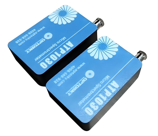
ATP1030 is an ultra‑compact, high‑resolution spectrometer covering 190–1100 nm. With a 1024‑pixel CMOS detector, adjustable integration time down to 1 ms, and USB‑powered design, it delivers reliable performance for applications like online water analysis, color measurement, handheld instruments, and Raman spectroscopy.
Product Recommendation | ATP1030 mini spectrometer Spectrometer

Vis-NIR transmission spectroscopy enables non-destructive identification of infertile duck eggs before incubation, achieving >95% accuracy. By detecting spectral fingerprints (e.g., 836 nm peak for fertile eggs), this method reduces energy waste and improves hatch rates, offering a low-cost, high-throughput solution for modern poultry farming.
Application case | How Spectral Technology is Transforming Duck Egg Farming