
Introduction to Spectrometer Detectors
author: Eliza
2024-10-10
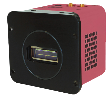
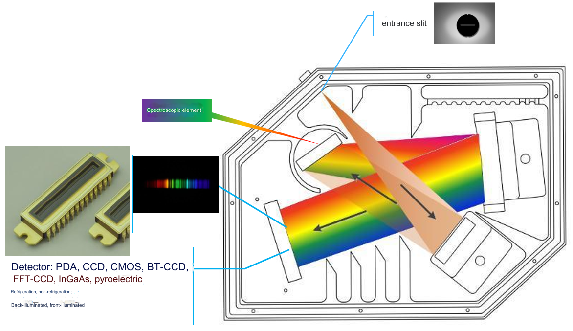
In the spectrometer, as shown in the figure, the detector is one of the core components used to detect and analyze spectral signals of different wavelengths separated by the dispersive element. It determines the instrument's sensitivity, signal-to-noise ratio, dynamic range, maximum operating wavelength range, and other performance characteristics. It is also a major cost component of the spectrometer.
According to their working principles, detectors can be categorized into various types, such as Photomultiplier Tubes (PMT), Photodiodes (PD), Single-Photon Detectors, Charge-Coupled Device (CCD) detectors, Complementary Metal-Oxide-Semiconductor (CMOS) detectors, Photodiode Arrays (PDA), Pyroelectric Detectors, and Cadmium Mercury Telluride (HgCdTe) detectors, among others.
The selection of detectors in a spectrometer is crucial and is usually based on factors such as wavelength range, detection sensitivity, and resolution requirements. For the ultraviolet-visible range, Si-based detectors are typically used, such as Si-based CCD detectors and CMOS detectors. For the near-infrared range, InGaAs detectors are generally chosen. For the mid to far infrared range, MCT detectors or pyroelectric detectors may be considered.
Part 01: Si-Based Detectors
Si-based Charge-Coupled Devices (CCD) and Complementary Metal-Oxide-Semiconductor (CMOS) detectors are two types of quantum detectors based on silicon materials, offering similar sensitivity in the visible spectrum, approximately ranging from 200 to 1100 nanometers. Both types of detectors are widely used in fields such as scientific imaging, industrial inspection, and biomedical applications.
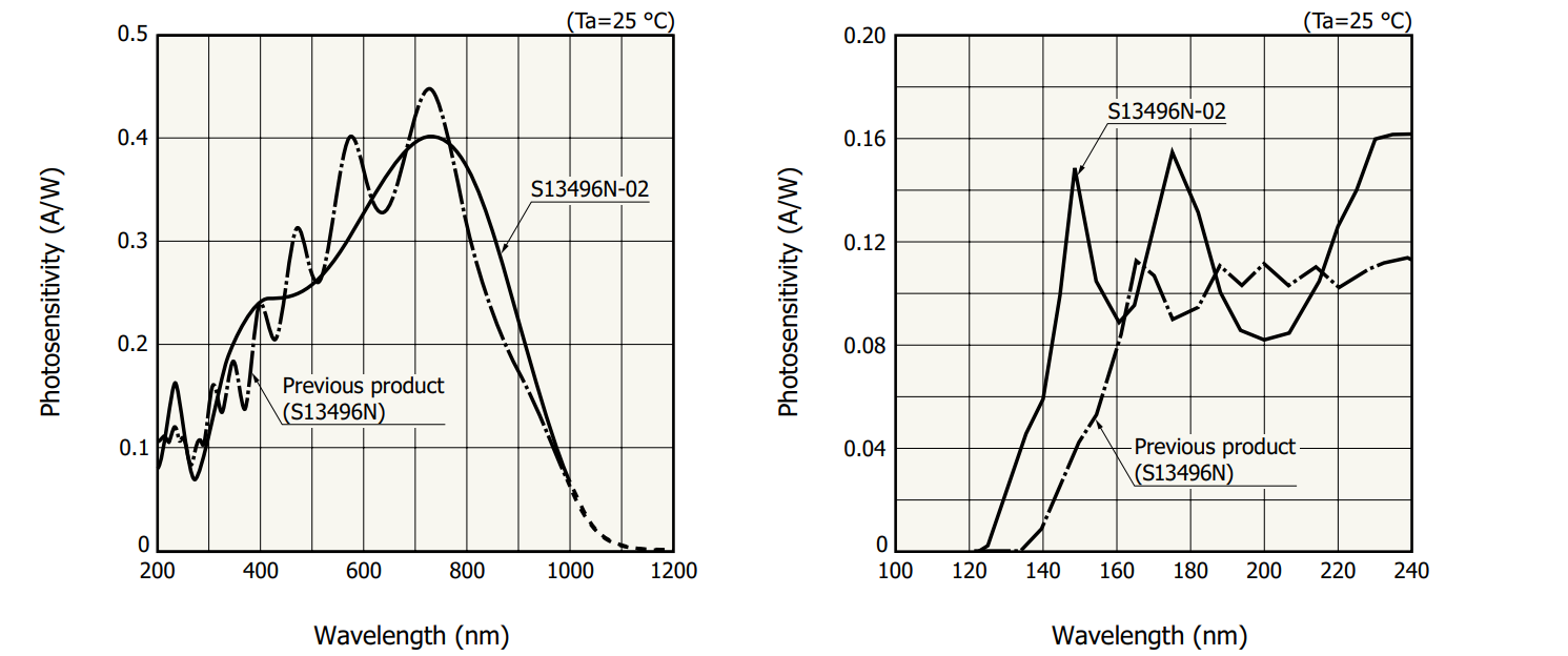
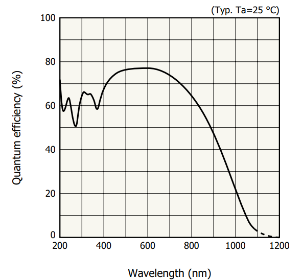
Figure 3: Spectral Response Curves of Si-Based CCD and CMOS Detectors
The basic working principle of CCD detectors involves the photoelectric effect, where incident photons are converted into electrons. Charge accumulates in each pixel, which is then read out by control circuits to form a digital image.
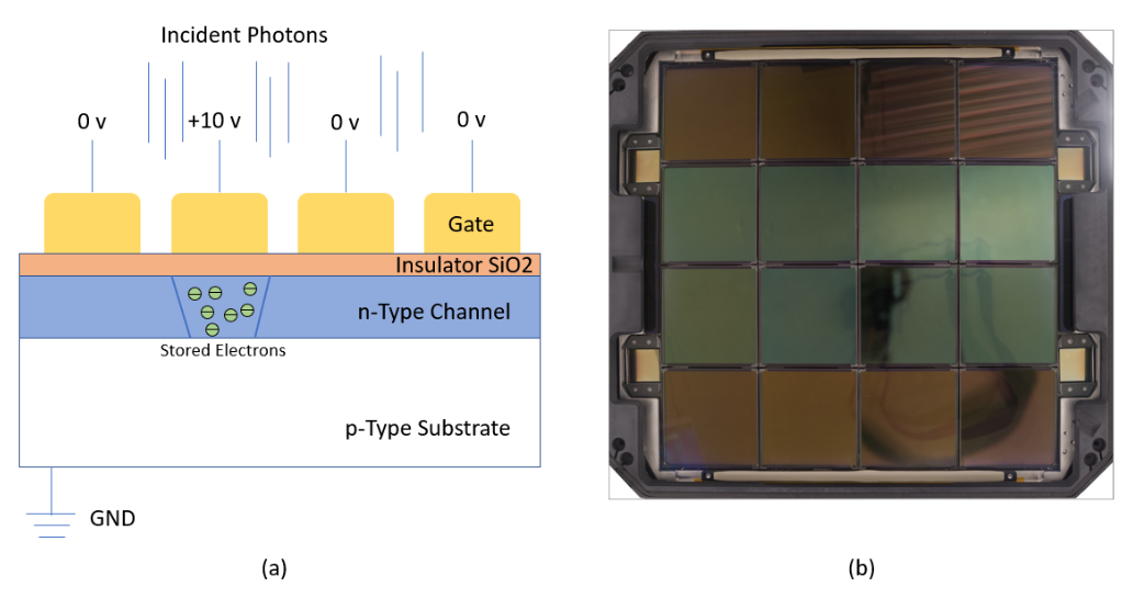
Figure 4: Structure of CCD Detectors
Commonly found in the market, Si-based CCD detectors consist of a silicon substrate and an epitaxial layer. By etching integrated circuits onto the silicon surface, a pixel array is formed. When photons strike the CCD surface, electrons are generated in each pixel in proportion to the light intensity. These electrons are then continuously transferred to the next pixel and accumulated until the exposure ends, at which point the charges from all pixels are read out at once.
CCDs offer high signal-to-noise ratios and dynamic ranges, making them ideal for spectral measurements across the ultraviolet to infrared range (180–1100 nm). Back-illuminated CCDs are particularly suited for the ultraviolet range, exhibiting excellent sensitivity and high resolution.
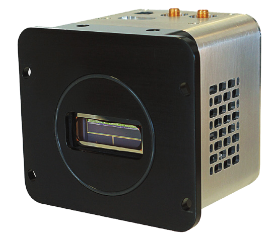
Characteristics of CCD Detectors
- High Sensitivity and Low Noise: CCD detectors excel in detecting weak signals with minimal background noise.
- Slow Readout Speed: Pixels are read sequentially, resulting in slower readout speeds and limited frame rates.
- Complex Manufacturing Process: Requires overlapping gate technology, leading to higher costs and power consumption.
CMOS Detector
A CMOS detector is a solid-state optoelectronic detection device manufactured using Complementary Metal Oxide Semiconductor (CMOS) technology.
Compared to CCD detectors, CMOS detectors do not transmit all sensor pixels through a single output node, an amplifier, and an analog-to-digital converter (ADC) as CCDs do. In CMOS technology, each pixel on the detection surface has its own miniature capacitor and amplifier, allowing for parallel operation through an ADC on each column. This enables all converters to work simultaneously, allowing for the readout of all pixels across the detection surface rather than just a single pixel.
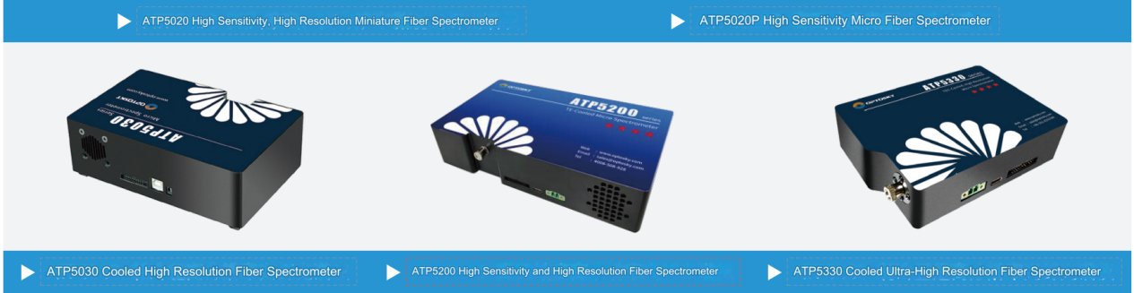
Figure 6. Optosky Line-Array CMOS Spectrometer
Features of CMOS Detectors
- CMOS detectors achieve a greater dynamic range and higher data throughput by integrating the readout electronics into the sensor chip.
- Known for their efficient energy usage, CMOS detectors only require current during state transitions, resulting in lower power consumption and reduced costs.
- With their rapid readout capability, CMOS detectors are ideal for high-speed imaging applications, such as video surveillance and motion capture.
Currently, due to the rapid readout, low power consumption, low cost, high integration, and high sensitivity of CMOS technology, line-array CMOS detectors are widely used in Optosky's micro/high-performance fiber optic spectrometers (180-1100 nm), effectively meeting various application requirements for customers.
Part 02: InGaAs Detectors
InGaAs detectors are high-performance optoelectronic devices widely used in various applications within the short-wave infrared and near-infrared spectral ranges. Their main features include high sensitivity, low noise, high quantum efficiency, and broad spectral response capabilities.
InGaAs detectors are high-performance optoelectronic devices widely used in various applications within the short-wave infrared and near-infrared spectral ranges. Their main features include high sensitivity, low noise, high quantum efficiency, and broad spectral response capabilities.
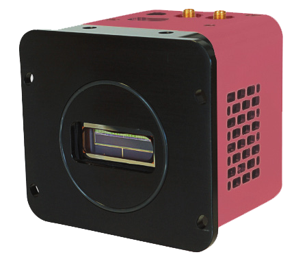
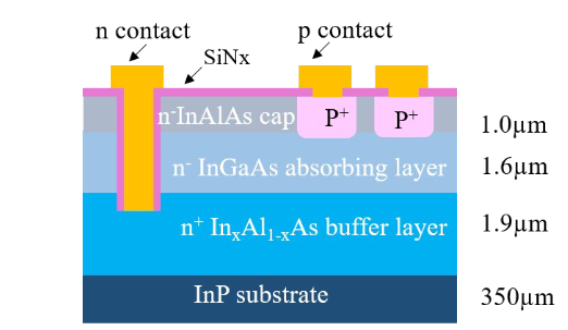
Figure 7. Structure of Planar InGaAs Detectors
From a materials and technology perspective, InGaAs detectors are typically grown using Molecular Beam Epitaxy (MBE) to create the epitaxial layers, which are then processed into junctions through techniques like diffusion doping. These detectors can achieve spectral responses from 0.9 μm to 2.5 μm and even longer wavelengths.
In terms of performance, InGaAs detectors exhibit high peak detectivity and quantum efficiency, especially in the near-infrared range around 1 to 1.7 μm. Additionally, by optimizing material growth parameters and surface passivation processes, the dark current density can be significantly reduced, enhancing the overall performance of the detectors in terms of signal-to-noise ratio and dynamic range.
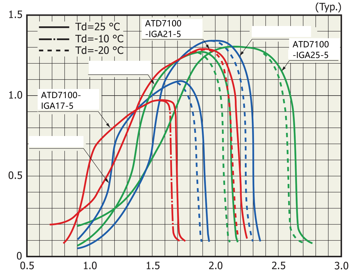
Figure 8. Optosky Cryogenically-Cooled InGaAs Detectors
Leveraging the high quantum efficiency and low noise levels of InGaAs detectors in the near-infrared range, Optosky integrates these detectors into infrared spectrometers covering the 900-2500 nm wavelength range. Depending on the specific requirements of the photosensitive surface, Optosky offers various configurations of detectors, including cryogenically-cooled single-unit InGaAs detectors, cryogenically-cooled line-array InGaAs detectors, and cryogenically-cooled planar InGaAs detectors.
Part 03: Pyroelectric Detectors
Pyroelectric detectors primarily consist of pyroelectric crystals (such as Nickel Niobate LT, PZT materials, and LN crystals), absorbers, electrodes, and circuitry. When the surface of the pyroelectric crystal absorbs infrared radiation, it generates a pyroelectric voltage signal due to the temperature increase. This signal is amplified by a preamplifier and sampled and held by a peak hold circuit, ultimately outputting a corresponding electrical signal.
Additionally, to enhance detection accuracy and suppress interference, synchronous trigger gating circuits and digital display technologies are commonly employed. During operation, the detector modulates a constant infrared radiation source to produce alternating radiation, causing corresponding temperature changes in the crystal and outputting an electrical signal. The detector window is typically made from specially vacuum-coated semiconductor silicon wafers, which adjust the infrared transmittance.
This type of detector has an extremely wide response range (0.1-100 µm), covering the spectrum from visible light to the mid- and far-infrared ranges, and can operate at room temperature, making it widely used in infrared spectrometers.
Part 04: Cadmium Mercury Telluride Detectors
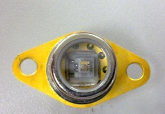
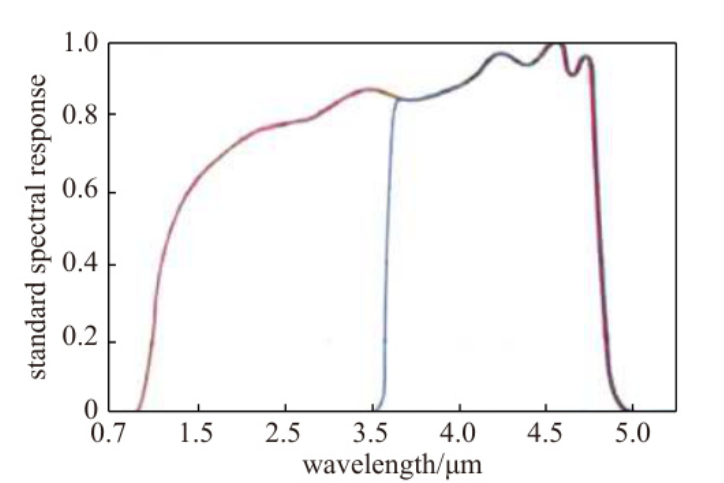
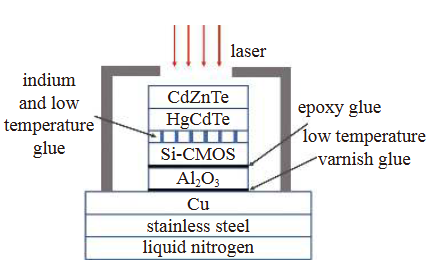
Figure 9. MCT Detectors
Mercury Cadmium Telluride (MCT) detectors are optoelectronic devices based on HgCdTe materials, operating on the principle of the photoelectric effect. When infrared light strikes the MCT semiconductor material, electron-hole pairs are generated. Under the influence of an external electric field, these electrons and holes move in opposite directions, converting the optical signal into an electrical signal for analysis and detection.
MCT detectors offer multiple advantages, including high sensitivity, fast response times, and a wide spectral range, covering the mid-infrared band from 1 to 15 μm. When paired with low-temperature cooling circuits, they provide optimal signal-to-noise ratios and response speeds, making them suitable for integration into Optosky's mid-infrared spectrometers.
Part 05: Indium Arsenide / Lead Sulfide Detectors
Lead Sulfide (PbS) detectors are optoelectronic devices based on PbS materials, featuring several excellent characteristics. Depending on different research and application needs, PbS detectors can be classified into traditional, quantum dot, and homojunction P-N types.
Although traditional PbS detectors have slower response times and can be easily damaged in high-temperature or bright light environments, they typically operate at room temperature with a wavelength range of 0.8-3.3 μm. Their simple structure and lower costs make them primarily suitable for infrared detection in the 1-3 μm range.
Indium Arsenide (InAs) detectors are an important type of infrared detector, characterized by:
- High Quantum Efficiency: The InAs/GaSb type-II superlattice material has a unique band alignment that provides high quantum efficiency and low dark current.
- Wide Wavelength Response Range: By adjusting the composition of the InGaAs absorption layer, a bandgap range of 0.35 eV to 1.43 eV can be achieved, covering different spectral regions.
- High-Temperature Operating Capability: InAs/GaSb materials can function at elevated temperatures while maintaining the advantages of simple III-V semiconductor processing.
For the 1-3 μm spectral range, Optosky offers infrared spectrometers equipped with PbS/InAs detectors for customer selection. PbS detectors are suitable for low-temperature applications, while InAs detectors are recommended for high-temperature environments.
Part 06: Spectrometer Detector Parameters
- Maximum Wavelength Range: The maximum operational range of the detector determines the spectrometer's maximum operational range;
Si: 180-1100 nm
InGaAs: 0.9 - 2.5 μm
- Quantum Efficiency/Sensitivity: The primary factor influencing the sensitivity of the spectrometer;
- Dynamic Range: Determines the dynamic range of the spectrometer.
Signal-to-Noise Ratio: Determines the signal-to-noise ratio of the spectrometer.
- Cooling: Indicates whether cooling is available and the achievable cooling temperature; effective cooling can significantly reduce dark current and readout noise, enhancing the stability of the spectrometer's operation.
- Response Time: Influences the sampling speed of the spectrometer.
Optosky offers various detector configurations tailored for different application scenarios and spectral ranges.
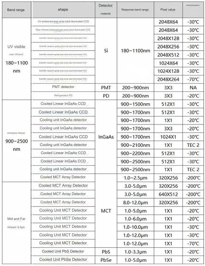
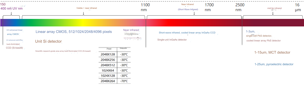
Refer to the detector-spectral range comparison table, where customers can select the appropriate model based on their actual needs!
Introduction to the optical path of a spectrometer
Fundamentals of Grating Knowledge Sharing
Related Article

The ATP7810 is a wide-band, high-resolution infrared grating spectrometer covering up to 0.9–5 μm. Featuring a motorized rotating grating, multiple detector options (InGaAs/MCT), and flexible interfaces (SMA905 or free space, USB/UART control), it delivers high SNR and stability for absorption/reflection/transmission spectroscopy, laser wavelength testing, and fiber optic sensing.
New Product Recommendation | ATP7810 Ultra-Wide Range Infrared Spectrometer Series

This study uses the ATP5200P UV-Vis spectrometer to investigate xanthate adsorption on chalcopyrite surfaces. By analyzing absorbance at 300 nm under controlled pH and temperature, the method optimizes flotation conditions for copper recovery, enabling real-time, sensitive detection of adsorption mechanisms in non-ferrous mineral processing.
Using the ATP5200P Spectrometer to Unravel Xanthate Adsorption and Separation Mechanisms

ATP1030 is an ultra‑compact, high‑resolution spectrometer covering 190–1100 nm. With a 1024‑pixel CMOS detector, adjustable integration time down to 1 ms, and USB‑powered design, it delivers reliable performance for applications like online water analysis, color measurement, handheld instruments, and Raman spectroscopy.
Product Recommendation | ATP1030 mini spectrometer Spectrometer

Vis-NIR transmission spectroscopy enables non-destructive identification of infertile duck eggs before incubation, achieving >95% accuracy. By detecting spectral fingerprints (e.g., 836 nm peak for fertile eggs), this method reduces energy waste and improves hatch rates, offering a low-cost, high-throughput solution for modern poultry farming.
Application case | How Spectral Technology is Transforming Duck Egg Farming