Application | Spectrometer Sensors in Film Thickness Measurement.
The measurement of film thickness is a critical technical issue in many fields, particularly in microelectronics, optics, and semiconductor manufacturing. Different film thickness ranges and material characteristics require different testing methods.
1. Film Thickness Measurement Methods
The development of film thickness measurement technologies has progressed through several stages, from early simple methods to modern high-precision techniques, playing an important role in material science and industrial applications.
Early methods primarily relied on optical microscopes and electron microscopes. While these could provide some thickness information, they generally lacked sufficient precision and resolution, especially at the nanoscale. As technology advanced, non-contact measurement methods became mainstream.
Choosing the appropriate measurement method depends on the specific film material, thickness range, and application requirements. For instance, in semiconductor manufacturing, ellipsometry and laser interferometry are widely used due to their high precision, while in tribology research, ultrasonic reflection methods offer non-invasive field measurement capabilities.
Interferometry, one of the most common non-contact methods for film thickness measurement, is widely used in micro- and nanoscale applications, such as measuring coatings on PCB boards, semiconductor films, and other thin materials. These samples are often thin, typically in the micron or nanometer range, and generally consist of transparent films, where the thickness significantly affects their performance and application, requiring high measurement precision (nanometer level).
2. Principle of Spectrometer Sensor for Film Thickness Measurement
When light strikes the surface of a thin film, interference occurs between the light reflecting from the film's surface and the light reflected from the substrate beneath, due to the difference in refractive indices and extinction coefficients of the film and the substrate. This interference causes a phase difference in the reflected light, resulting in interference fringes in the spectrum. By analyzing these fringes, the film thickness can be calculated.
As shown in the diagram, a thin film with a refractive index η (complex refractive index η = n + ik) and thickness d is deposited on a substrate with refractive index n1, while the refractive index of air is n0. When a light beam with amplitude A is incident at angle θ (in practice, θ is usually small and its effect on the measurement is negligible, so it is often assumed to be normal incidence, i.e., θ = 0°), refraction and reflection occur. The refracted light undergoes multiple reflections within the film, ultimately producing a series of reflected light on the top surface.
By analyzing these reflected light patterns (interference fringes), the thickness of the film can be determined. This principle is applied in various spectrometer sensors, including those using white light interference and optical thickness gauges, providing precise measurements of films at the micro- and nanoscale.
According to the principle of multi-beam interference, the complex amplitude of the reflected light can be expressed as:
r1 and r2 are the reflectivities at the air-film interface and the film-substrate interface, respectively. According to the interference principle, the phase difference between two adjacent beams, caused by the optical path difference, can be expressed as:
The reflectance R can then be obtained as:
When the film absorption is very small, the variations in nnn (refractive index) and kkk (extinction coefficient) can be neglected. The maximum and minimum reflectance values occur at:
,m=0, 1, 2, ...
When white light is incident, the conditions for interference bright and dark fringes can be derived. These correspond to the positions of the spectral peaks and valleys in the white light interference spectrum.
The interference spectrum of reflected light from a glass film on a silicon substrate.
The thickness of the film can be calculated from the positions of the maximum and minimum points on the curve:
,
M is the number of interference fringes between two maxima or minima. M=1 indicates the distance between two adjacent maxima (peaks) or minima (troughs).
The film thickness can also be calculated using the wavelengths of adjacent peaks (λ1) and troughs (λ2) as follows:
In actual measurements, multiple film thickness values are obtained by using several sets of corresponding peak and trough wavelengths. The average value is taken to reduce measurement errors.
Due to the effect of different film thicknesses on the optical path difference, the relationship between the interference spectrum and the film thickness is as follows:
03 Spectrometer Sensor Film Thickness Measurement Solution
The application of spectrometer sensors in film thickness measurement is also based on the principle of white light interference. By analyzing the interference peaks in the reflected spectrum, the film thickness can be determined. The required spectrometer configuration varies depending on the film thickness, such as the choice of wavelength range and resolution.
Specifically, the spectrometer sensor transmits light from a stable light source through a Y-type optical fiber to the sample surface, collects the reflected light, and then transmits the optical signal to the spectrometer for processing. The spectrometer software analyzes and generates the reflected spectrum. Based on the relationship between film thickness and the wavelengths of the spectrum's peaks and troughs, along with known material optical parameters (such as refractive index and extinction coefficient), further data processing allows the film thickness to be calculated.
This method is characterized by high precision and fast measurement, making it suitable for industries such as semiconductors, coating, panels, and functional films.
Another advantage of the spectrometer sensor is its non-contact measurement capability, which prevents damage to the thin film during the measurement process. Additionally, its compact design and small size make it ideal for in-situ, real-time monitoring of film thickness. This method allows for continuous monitoring of film thickness and is applicable not only for single-layer films but also for multilayer film thickness measurements.
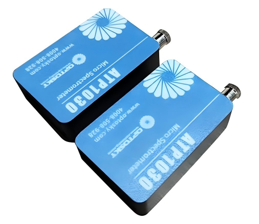
ATP1030 Mini spectrometer
Application of Spectrometer Sensors in Fluorescence Spectroscopy
Related Article